DIGITAL PRODUCTS DRAWINGS
DAY SOLAR INVERTER SCHEMATIC DIAGRAM OF CHINA PCB


Product Summary +
DAY SOLAR INVERTER SCHEMATIC DIAGRAM OF CHINA PCB
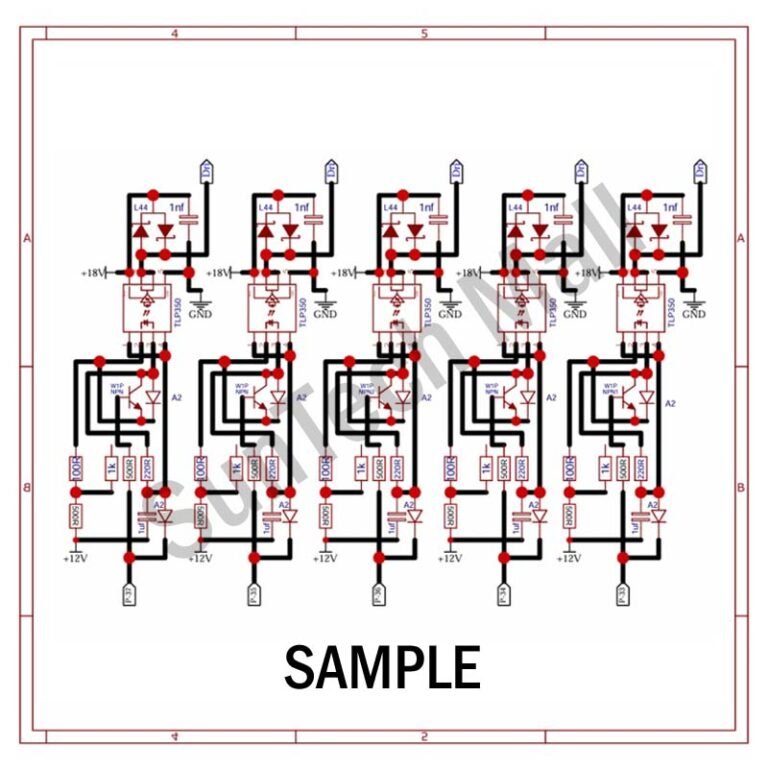
The China DAY solar inverter is a popular device for converting solar energy into usable electricity. Its schematic diagram shows key parts like components tracks and board connections.
DAY SOLAR INVERTER SCHEMATIC DIAGRAM:
A solar inverter’s schematic diagram shows its main parts.
The DAY Solar Inverter Schematic Diagram is crafted by expert engineers to meet the demands of modern solar energy systems. Its precise layout and detailed annotations empower users to understand, build, or repair solar inverters with ease. Compatible with high-quality PCB manufacturing standards, this schematic ensures electromagnetic compatibility, thermal management, and mechanical stability, delivering efficient and safe power conversion. Perfect for professionals and hobbyists alike, this diagram is your key to unlocking the full potential of solar energy.
The schematic provides a clear layout of critical sections, including the DC-to-AC conversion, power supply, booster, output, and MPPT charger circuits, enabling efficient troubleshooting, installation, and system optimization. Designed for 5KVA and 6KVA solar inverters, this diagram ensures precise wiring connections, robust safety mechanisms, and optimal performance, making it an essential tool for building or maintaining reliable solar energy systems. Whether you’re a professional installer or a DIY enthusiast, this schematic simplifies complex circuit designs, helping you harness clean, renewable energy with confidence.
Customer Reviews
Be the first customer to review this product.
Pending reviews will appear after approval.